There are a variety of inexpensive (<$100) entry level near-field probes available from the usual suspects, however I've been dissuaded from purchasing them for the following reasons:
- Fly by night operations: How long will this random ebay item be available? Will there be any other source for this model of probe? Where did this come from anyway? The seller certainly has no association with the designer.
- Documentation: Most of these things lack a named manufacturer and model number. What kind of response and characteristics was it designed to have? At best you get a grainy jpg showing a possibly fake frequency response curve with unlabeled axis. How is it different from other similar models from a hundred other nameless ebay vendors?
- Design: Were these things actually...designed? All the cheap probes are fabricated on 2 layer PCB stackups and lack adequate electrical shielding. Some of these traces look like they might be 50 ohm but others definitely aren't. Without documentation there's no way to verify the intent of the designer. Maybe some of these probes are okay but none of them show it and I would have to buy them all to check.
I aim to solve some of these problems with Open Field Probe. Minimal effort is required to improve the basic designs. At the very least you will be able to download CAD files and gerbers and know where they came from.
Near field probes detect time-variant electric and magnetic fields in the "near field" around an electrical device, ie the region within one wavelength where normal radiative effects have not yet been expressed. Energy can be strongly coupled into probe devices at this range with a high degree of spacial resolution which aids in pinpointing sources of electromagnetic emissions which can later lead to certification failure. Alex Whittimore hosted a great workshop on the process as part of the 2020 Remoticon.
The two types of probes implemented in this project are of the E and H field type. An E-field probe is simply a short stub of copper which capacitively couples to a trace or wire under test and an H-field probe is a loop which has a current induced within it by the magnetic fields surrounding the trace or wire under test. These probes are connected to a low-noise high-gain amplifier which in the case of the H-field probe converts the current into a voltage using the amplifier's input impedance. The amplified signals are then send to a spectrum analyzer, oscilloscope or other piece of test equipment.
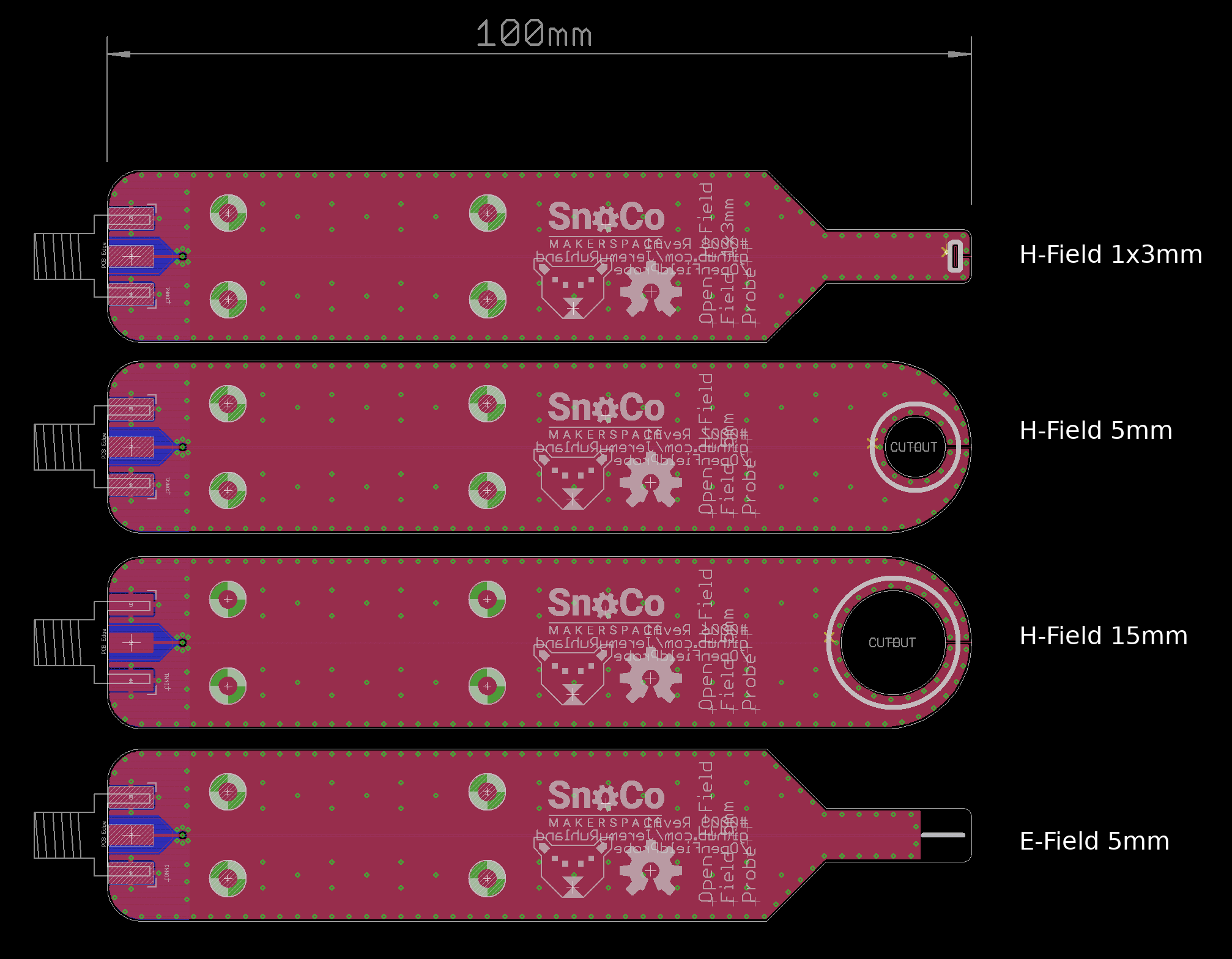
The PCBs are designed to be fabricated on JLCPCB's 4-layer JLC7628 stackup. The top and bottom layers are continuous ground pours stitched together on the edges by a via fence. This shields the internal signal carrying trace from unwanted electrical noise. In the case of the E-field probe the shielding is pulled back near the tip where the E-field coupling takes place and in the case of the H-field probe there is a narrow slit made in the shield at the tip of the probe which permits external magnetic fields to induce a current in the loop formed by the signal trace but not in the shielding layers.
In both probe types the signal is picked up by an internal trace on layer 2 which is modeled as a stripline, sized to have a characteristic impedance of 50 ohms. The H-field probe has one end of its pickup loop terminated into the ground shield by a via. The center of the pickup loop is cut out to minimize dielectric losses in the FR4 material.
In order to connect to the center pin of the SMA connector the signal trace must transition to the top layer through a via at the far end of the probe. Although the prepreg thickness between the top and second layer is only 0.2mm and the full length of the via (PCB thickness) is 1.52mm the transmission line properties of the via were modeled as a coaxial cable formed by the via itself, the FR4 substrate and a surrounding ring of vias connected to the ground shield layers. Via sizing and ring spacing was calculated to maintain a characteristic impedance of 50 ohms.
The transition of the signal trace to the top layer occurs at the edge of a ground plane pour on layer 2 which extends under the SMA connector and is heavily via stitched into the top and bottom layer ground shield pours. The segment of the signal trace between the via and SMA connector center pin pad is modeled as microstrip with a characteristic impedance of 50 ohms. The top layer ground shield pour is pulled back from the signal trace to minimize coplanar waveguide effects on the trace impedance.
The SMA connector is designed to have a characteristic impedance of 50 ohms and vias are used to stitch the connector ground pads into the shielding layers. A 50 ohm coaxial cable is used to connect both probe types to an inexpensive +30dB LNA which is designed for RTL-SDR applications. Depending on the exact measurement device used this amplifier may not be required. RTL-SDR units should be sensitive enough to detect signals without further amplification. The LNA is powered at 5V by the USB port on the front of my oscilloscope. Common mode currents in the coaxial cable are suppressed using a clamp-on ferrite bead.
The input and output impedance of the LNA is 50 ohms which requires feedthru termination of my oscilloscope input. This is accomplished using an inexpensive BNC terminator, but depending on the test equipment an internal 50 ohm terminator may be available.
Sch and brd files are designed in Eagle CAD 6 but should be forward compatible to more recent versions.
Each board's gerbers are stored in a seperate folder and are submittable to fab.
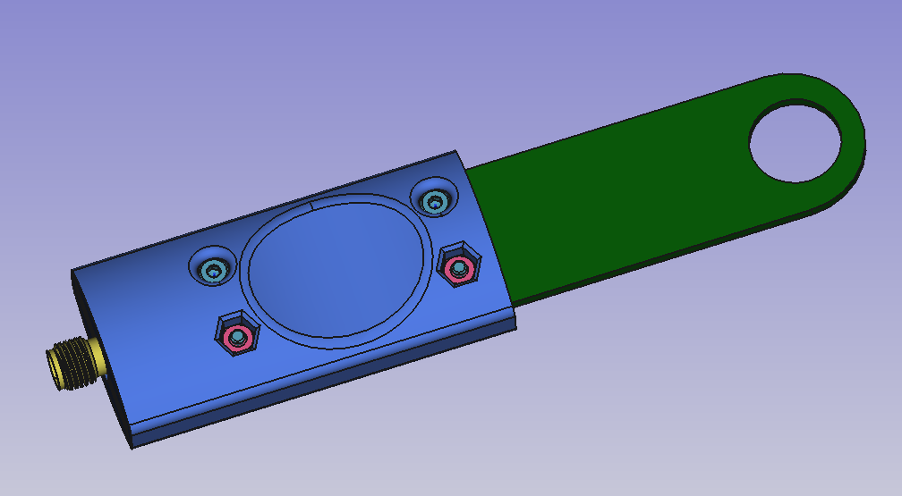
The CAD folder contains a 3D printable clamshell grip for the probe, designed in FreeCAD0.19. Print out two copies and fasten with four M2 screws/nuts.
TBD
TBD

